NFF (CWB) Services
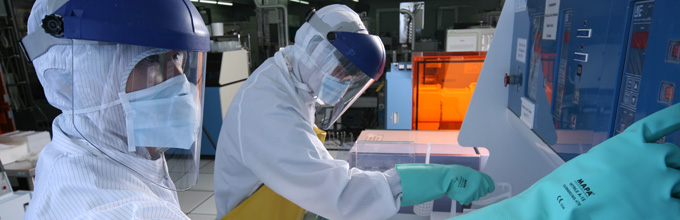
As one of the key facilities at HKUST, we provide services to the faculty members of different departments for teaching and research purposes. We also provide services to other tertiary institutions and collaborate with the private sectors. The aim is to seek opportunities to explore and develop advanced nano-electronics technologies. We offer services in the following areas:
- 3D Nano-electronics Devices
- Display Technology
- Micro-sensors
- Micro-Electro Mechanical System
- Silicon Photonics Technology
- Power Semiconductor Devices and Technology
- Advanced Packaging Program
- Advanced Process Module Development
- Gene Chip
- Compound Semiconductor Technology
There are two ways to use NFF (CWB) services. One is to apply to become an NFF (CWB) user and another one is to submit a work request form to NFF (CWB) for facility services. The two ways have different procedures to go through.
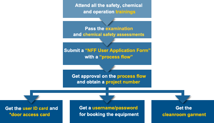
Applying to become an NFF (CWB) user
Submitting a work request to the NFF (CWB)
A job request for wafer processes

A job request for mask making

Click HERE for more details about mask making
NFF (CWB) Charging Scheme
There is one charging rate for HKUST users and two charging rates for non-HKUST users.
For more details, please click HERE.