Wet Etching and CMP Module
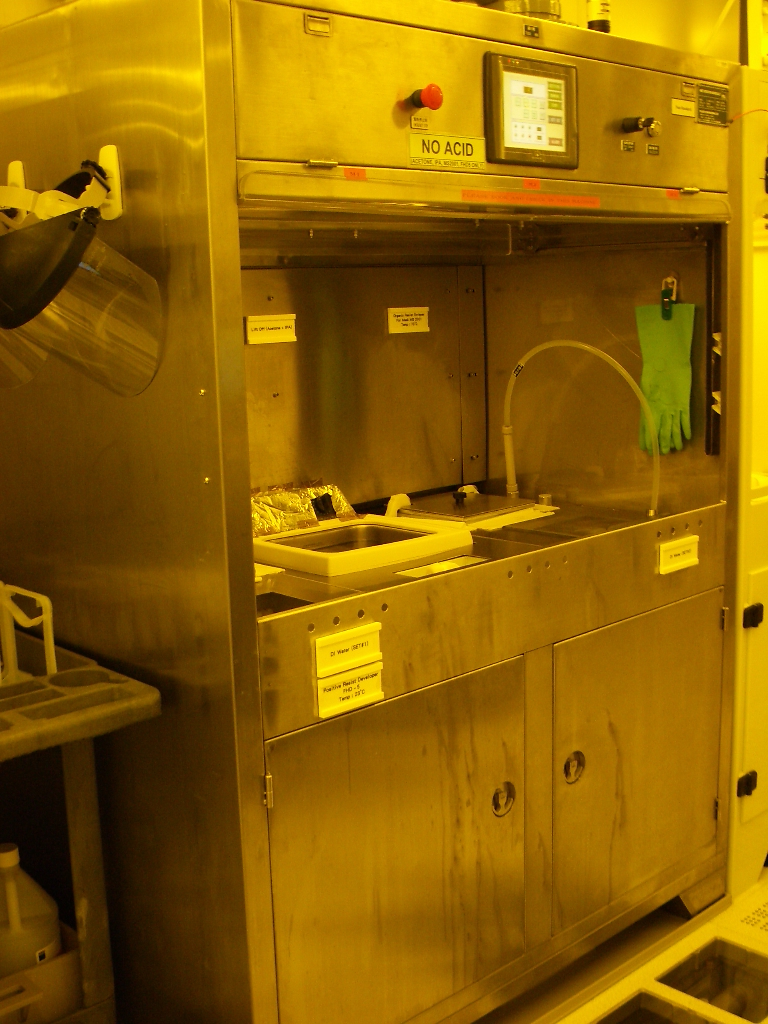
Wetstation A, B, C, D, E, F, G and H
Clean/Semi-clean/Non-Standard
WET-A1 to WET-A3, WET-B1 to WET-B3, WET-C1 to WET-C3, WET-D1 to WET-D4,
WET-E1 to WET-E4, WET-F1 to WET-F3, WET-G1 to WET-G2, WET-H1 to WET-H3
Specifications
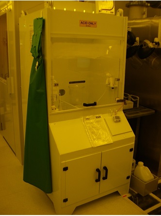
| Wet processing | : | Silicon Etch using KOH / TMAH (25%) Photoresist Strip / ITO Etch Aluminum Etch / Pad Oxide Etch Oxide / Nitride Etch Wafer Cleaning (RCA) Wafer Cleaning (Piranha Clean) Solvent Cleaning |
|---|
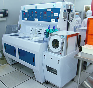 Wetstation A and B |
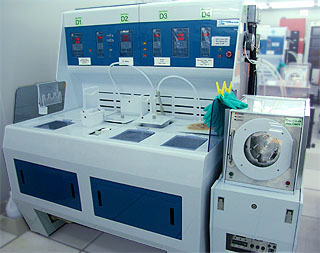 Wetstation C and D |
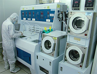 Wetstation E and F |
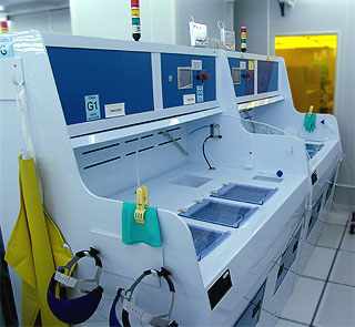 Wetstation G and H |
Wetstation M (WET-M1 to WET-M3)
Non-Standard
Specifications
| MS2001 Resist Stripper |
| FHD5 Manual Developer |
| Quick Dump Rinsers |
| Small samples up to 6” |
Wetstation O (WET-O1)
Non-Standard
Specifications
| Hydrochloric Acid Etch Prior E-Beam Metallization |
| DI Water Gun for rinse |
| N2 Gun for dry |
| Small samples up to 6" |
Wetstation W, X, Y and Z (WET-W1 to WET-W2, WET-X1 to WET-X2, WET-Y1to WET-Y2, WET-Z1 to WET-Z2)
Clean/Semi-clean/Non-Standard
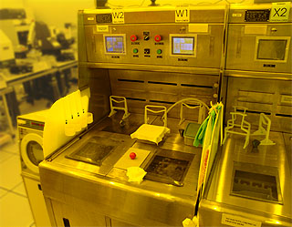
Specifications
| MS2001 resist stripper |
| FHD5 manual developer |
| Quick dump rinsers |
| Small samples up to 6" |
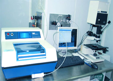
USI Wafer Cleaner (CMP-2)
Clean
Specifications
| Wafer surface scrubbing for pre-CMP and post -CMP process |
| Fully automatic microprocessor control |
| Completely enclosed chamber for washing, rinsing and drying |
| 4" wafer cleaning |
| 9" brush travel |
Silicon Grinder (CMP-3)
Semi-Clean
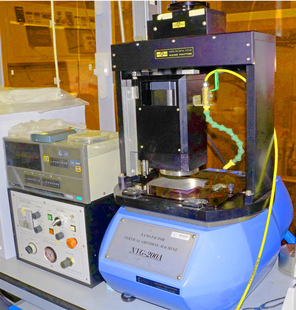
Specifications
| Mechanical grind for Silicon Oxide or Silicon using diamond wheel |
| >5mm2 to 4" wafer size |
| 100-800um wafer thickness |
Buehler Polisher #1 (CMP-4)
Semi-Clean
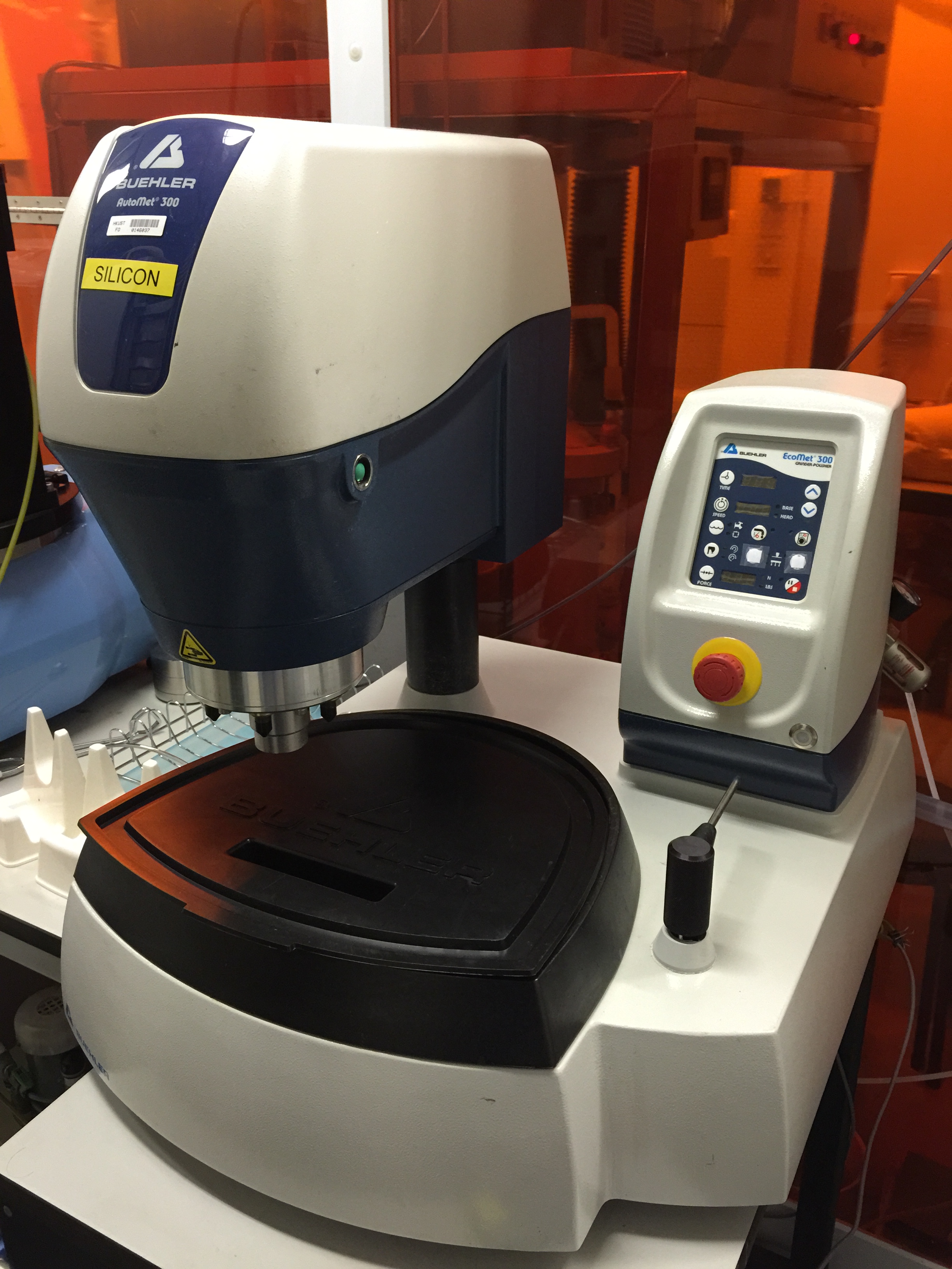
Specifications
| Polished for Silicon, Silicon Oxide or Silicon Nitride |
| >5mm2 to 4" wafer size |
| 100-800um wafer thickness |
Buehler Polisher #2 (CMP-5)
Non-Standard
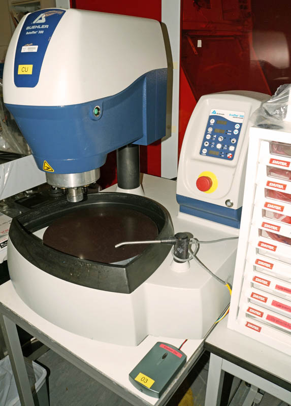
Specifications
| Polished for Copper, CNT, Silicon, Silicon Oxide or Silicon Nitride |
| >5mm2 to 4" wafer size |
| 100-800um wafer thickness |
GnP CMP (CMP-6)
Clean
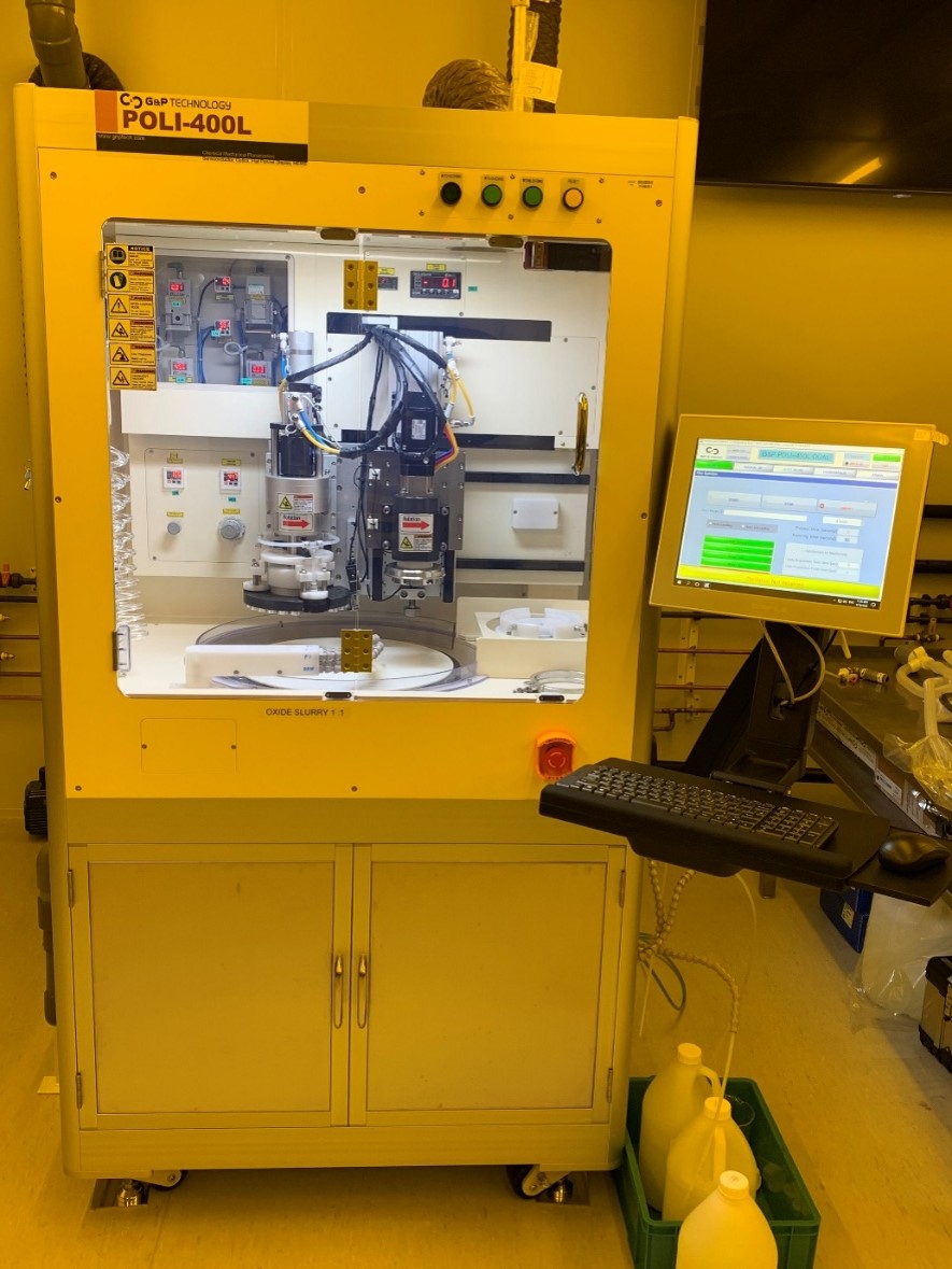
Specifications
| Equipment model | : | POLI-400L |
|---|---|---|
| Polishing materials | : | Silicon dioxide or Polysilicon |
| Sample Size | : | 1"x1" or 4" |
| Wafer Thickness | : | 400-550 µm |
| Wafer Carrier | : | Membrane style with floating ring |
| Polishing platen and wafer carrier speed range | : | 30-200 rpm |
| Oscillating Arm Pad Conditioning |
Copper Electroplating (EP-1)
Non-Standard
Specifications
| Copper Electroplating on 2" single side or 4" single/double sides wafer size |
| Ready for Copper Electroplating to fill the small trench 300-550um wafer thickness |