Modules in NFF (CWB)
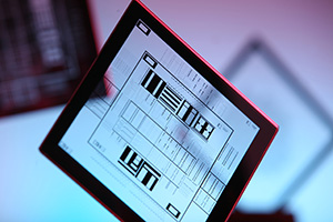
A photomask is typically a transparent fused glass blank covered with a pattern defined by chrome metal. A set of photomasks, each defining a pattern layer in nanoelectronic fabrication, is fed into a photolithography contact aligner or stepper and individually selected for exposure on a silicon wafer. In the case of the contact aligner, there is a one-to-one correspondence between the mask pattern and the wafer pattern. With the stepper, however, the pattern is projected and shrunk by five times onto the wafer surface.

Photolithography is the complicated process of transferring a pattern from a mask onto the surfaces of silicon wafers or any other substrates. Photolithography is in fact a highly refined version of photoengraving and is performed in a particle-free environment (the "yellow area"). The pattern is first transferred from the mask to a light-sensitive material called a photoresist. It is then transferred from the photoresist to the barrier material on the surface of the wafer by chemical etching or plasma etching.
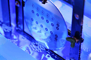
Chemical wet etching is the technique of removing any barrier material not protected by the hardened photoresist after the photolithography process using liquid-phase etchants. Etchants must be highly purified and filtered. Which etchant to use depends on the material to be etched. We have several specially designed wet processing stations and a wide variety of pre-mixed etchants to choose from.
The Chemical and Mechanical Polishing (CMP) process is a breakthrough technology in the manufacture of today's advanced semiconductor chips. It is a highly accurate process of flattening and smoothing the surface of a silicon wafer so that multiple layers of intricate chip circuitry can be built on it. The process is essential to maintaining a wafer's integrity, especially as the new generations of chips continue to shrink in size.
Thermal Diffusion and Ion Implantation Module
To fabricate nanostructures and nanodevices, various kinds of thin films are used. Thermal oxidation plays an important role in silicon device fabrication. It is a key process in modern semiconductor technology. Dielectric materials, such as silicon dioxide and silicon nitride, are mainly used for insulation and passivation. Low-Pressure Chemical Vapor Deposition (LPCVD) and Plasma-Enhanced Chemical Vapor Deposition (PECVD) are the most commonly used methods for thin film deposition. For high-K material, atomic layer deposition offers precise control of film thickness down to the atomic scale and excellent conformity even in high-aspect-ratio structures. Polysilicon acts as the gate electrode and device interconnection is achieved through silicide formation. The thermal process facilitates oxidation and thin film deposition in wafer processing. Other related processes are thermal annealing which enables us to study the properties of different materials or their structural performance as a function of temperature, thermal diffusion dopant activation, etc.
Ion implantation is the process by which impurities such as boron and phosphorous are introduced into a silicon wafer to control the majority-carrier type and resistivity of layers formed on the wafer. It is the primary method used to modify the electrical properties of wafers. Following ion implantation, a thermal diffusion or annealing process is needed to drive-in and activate the implanted dopants.

Dry Etching and Sputtering Module
Dry etching is one of the most critical processes in micro and nanofabrication. This process is also known as dielectric etching, polysilicon etching, or conductor etching, depending on the type of film that is removed from the substrate. Two basic steps are involved. In the pattern definition step, a lithography process is used to create the desired pattern on the photoresist. Then in the pattern transfer step, the required pattern is dry etched onto the silicon itself, or onto a deposited layer of insulating or conducting material. The most common form of dry etching is reactive ion etching (RIE), through which a highly anisotropic profile of the etched material can be obtained.
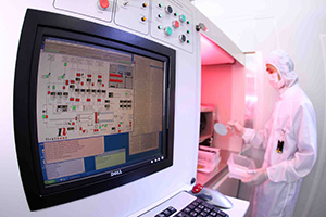
In-line process characterization for photolithography, etching, CMP, ion implantation and CVD enables us to monitor the machine performance and a number of key process control functions. We are equipped with many metrology systems providing non-destructive or destructive, real-time measurement of critical parameters. The effectiveness of the whole process can thus be monitored.
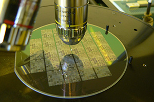
In-line process characterization for photolithography, etching processes, CMP, ion implantation and CVD processes enables us to monitor the machine performance and a number of key process control functions. We are equipped with many metrology systems providing non-destructive or destructive, real-time measurement of critical parameters. The effectiveness of the whole process can thus be monitored.